


How Does 224G SerDes Drive the Transition to 1.6T Optical Networking?

By doubling the single-channel electrical signal rate from 100 Gbps to 200 Gbps, the 8-channel electrical interface allows the system bandwidth to jump directly from 800G to 1.6T without increasing the number of physical channels. However, this doubling of the rate also brings a chain reaction, placing extremely stringent engineering requirements on signal integrity, equalization and signal processing algorithms, chip packaging technology, overall power consumption, and thermal management.
This article will look at how SerDes technology has evolved from 112G to 224G. It'll look at the design trade-offs and implementation challenges of the 8x200 Gbps electrical interface architecture behind 1.6T and provide a detailed examination of the implementation strategies for the 1.6T DR8 and 2xFR4 optical modules.
224G SerDes Overview: What is 224G SerDes?
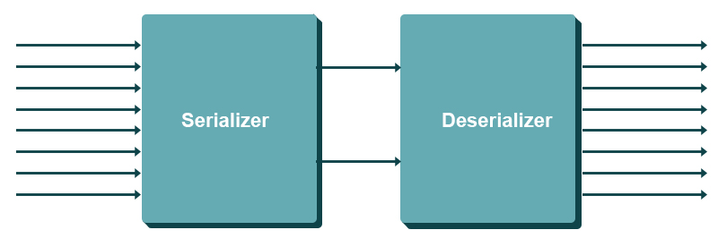
SerDes (Serializer/Deserializer) is a low-level high-speed interface technology. Its core task is to convert low-speed parallel data into high-speed serial signals within devices such as ASIC chips, and then restore it to parallel data at the receiving end. Through this serial-to-parallel conversion, high-speed devices such as switches, network interface cards (NICs), and optical modules can support high-frequency throughput of massive amounts of data without blindly piling on physical pins and wiring.
The industry calls this "224G SerDes", and it's a high-speed electrical interface designed for 224G-level PAM4 signal modulation. It's important to clear up one common misunderstanding: "224G" refers to a generational level of physical signal rate, but the net effective payload carried by a single channel isn't exactly 224 Gbps. Take the 1.6TAUI-8 interface, for example. This is defined in the OSFP MSA specification, and the underlying layer uses a 106.25 GBd 224G-PAM4 signal. The effective single-channel transmission rate is 200 Gbps.
How Can a 224G SerDes Support a 1.6T Network?
The shift from 112G to 224G SerDes essentially restructures the expansion logic of the electrical interface evolution towards 1.6T. Previously, increasing total bandwidth primarily relied on "adding physical channels," while 224G SerDes directly doubles the data-carrying capacity of a single-channel electrical signal from 100 Gbps to 200 Gbps.
The core architectural change is very direct: single-channel 100 Gbps → single-channel 200 Gbps.
Why is the 8×200 Gbps PAM4 architecture more scalable?
In the 800G era, an 8×100 Gbps architecture was sufficient to meet aggregated bandwidth requirements. If 1.6T still uses the single-channel 100 Gbps solution of 112G-PAM4, the entire system would have to be expanded to 16 electrical interfaces.
Doubling the number of channels means there's a lot more high-speed physical traces between the switch ASIC chip and the optical module. This really reduces the space for PCB routing and makes chip packaging, connector size, and overall integration way harder.
For OSFP host interfaces that still use an 8-channel design, the 1.6TAUI-8 specification provides a smooth evolution path without increasing the number of channels—directly crossing the 1.6T bandwidth threshold while maintaining the physical density of 8 channels.
How Does 8×200 Gbps PAM4 Achieve 1.6T?
The 1.6TAUI-8 mode defined by OSFP MSA uses 8 pairs of differential electrical channels, based on 106.25 GBd of 224G-PAM4 signal modulation. Each channel has a rated rate of 200 Gbps, and 8 channels in parallel provide a total bandwidth of 1.6 Tbps: 8 × 200 Gb/s = 1.6 Tb/s
At the host interface level, OSFP MSA has planned flexible PMD mapping combinations, including 1×1.6T, 2×800G, 4×400G, and 8×200G. It should be noted that these are specification-level mapping definitions; the specific offloading or direct connection mode supported by the device in actual deployment depends on the switch ASIC, optical module solution, underlying communication protocol, and specific firmware implementation.
The shift to 224G SerDes completely changed the scaling paradigm of 1.6T interconnects: instead of doubling the number of high-speed physical channels, the bandwidth of each channel is directly doubled.
Core Benefits and Engineering Challenges of 224G SerDes
The architectural benefits of transitioning from 112G to 224G SerDes are obvious, but doubling the baud rate also significantly increases the engineering challenges. Evaluating the practical value of 224G must be done objectively, balancing the technological benefits with the engineering challenges.
Higher Bandwidth Density
With the single-channel electrical signal rate jumping from 100 Gbps to 200 Gbps, the aggregate bandwidth doubles while maintaining the standard 8-channel electrical interface. Its core value lies not in adding more physical ports, but in dramatically increasing the bandwidth density per unit space. This is particularly crucial for space-constrained AI computing platforms—within a given chip package size, switch front panel space, and limited chassis volume, a single interface must handle a higher density of traffic throughput.
Halved Channel Number, but Dramatically Increased Electrical Design Difficulty
Compared to the equivalent bandwidth achieved through 16×100G, the 8×200G architecture requires half the physical channels, alleviating PCB congestion and packaging pressure caused by trace stacking. However, the trade-off is that the engineering tolerance of a single electrical channel is compressed to the extreme. There's been a big rise in the baud rate, and this has a really negative effect on high-frequency attenuation. Things like insertion loss, signal reflection, inter-channel crosstalk, via parasitic effects, connector mechanical deformation, and PCB dielectric loss can all directly threaten signal integrity. The OIF CEI-224G standard, which specifies various interconnect distances such as chip-to-module (C2M), emphasizes multi-layer collaboration—SerDes architecture, high-frequency traces, connector selection, and chip packaging must be refined as a system-level engineering process.
Power per Bit and Heat Dissipation Challenges
Basically, if you can double the single-channel rate, you should be able to reduce the power per bit (pJ/bit), because you'll get double the bandwidth with fewer physical channels. But this doesn't automatically mean that the optical module or the whole system will use less power. How much power is used depends on how complex the SerDes analog front-end and DSP algorithms are, how efficient the optical components are, and how much link loss compensation costs. The heat dissipation challenges that come with high power consumption are also a big concern. With the heat density per unit volume increasing dramatically, passive heat dissipation from the optical module casing alone is insufficient; the design of the module heatsink, optimization of the switch chassis airflow, and the overall system heat dissipation capacity must be considered together.
Signal integrity, equalization algorithms, and FEC are all connected. The electrical signal rate gets doubled, which directly erodes the eye diagram margin, and high-frequency losses severely distort the PAM4 signal, which was originally clear. To smooth out channel impairments, 224G systems must rely on more aggressive equalization algorithms and DSP signal repair capabilities at both the transmitter (Tx) and receiver (Rx) ends; at the protocol and link layers, a more robust forward error correction (FEC) mechanism is also needed to ensure the target bit error rate. The IEEE P802.3dj standards working group is currently defining 200G, 400G, 800G, and 1.6T specifications, with the core focus on a single-channel 200 Gbps electrical interface. This shows that 224G SerDes is more than just a replacement for an interface chip; it's a complete upgrade that includes SerDes, PCB routing, connectors, DSP, FEC, optical packaging, and thermal design.
224G SerDes Implementation in 1.6T Optical Modules
Mapping 224G-level SerDes to a specific 1.6T optical module architecture reveals its engineering value more clearly. In actual deployment, although the underlying systems are all based on 8 200G-PAM4 electrical interfaces to run at full 1.6T aggregate bandwidth, there is a clear divergence in the implementation path on the optical side: DR8 relies on parallel fiber technology, while 2×FR4 adopts a dual-path 4-channel wavelength division multiplexing (CWDM) architecture.
1.6T DR8 (Parallel Single-Mode Solution): It uses a Twin-port (2×800G) OSFP package, and inside there are two independent 4-channel parallel 200G-PAM4 optical links, with each one starting via a Dual MPO-12/APC interface. This supports a transmission span of up to 500 metres over single-mode fiber. This architecture does away with the insertion loss and assembly complexity of wavelength division multiplexing (WDM) components, making it perfect for high-bandwidth, high-density short-distance backbone direct connections within data centers.
1.6T 2×FR4 (Coarse Wavelength Division Multiplexing Solution): Also relying on 8×200G electrical interfaces to provide a total bandwidth of 1.6 Tbps, the optical side consists of two 4-channel FR4 sub-links. Each sub-link multiplexes four 200G-PAM4 optical signals onto a CWDM4 wavelength grid with a 1310nm window, transmitting and receiving via a standard Duplex LC (Dual Duplex LC/UPC) interface, achieving stable transmission over single-mode fiber up to 2 kilometers. Compared to multi-fiber parallel solutions, it significantly reduces fiber core resource consumption in medium- to long-distance or cross-data center scenarios.
These two typical designs show that the same 200G single-channel electrical interface technology can be used in different ways to create different optical implementation schemes: DR8 uses multi-fiber parallelism to support high-density short-distance interconnection within data centers, while 2×FR4 overcomes distance bottlenecks and reduces fiber core usage through wavelength division multiplexing. When planning the network, there are a few things to keep in mind, like specific conduit cabling assets, port splitting plans, and the parameter details in the product datasheet.
Conclusion
224G SerDes is establishing the underlying electrical paradigm for 1.6T high-speed networks—its core significance lies in maintaining the system's physical boundaries of 8-channel electrical interfaces through a single-channel 200G speed leap. However, translating this architectural advantage into reliable service computing power requires a collaborative engineering approach across the entire chain, encompassing SerDes analog front-end, channel integrity, high-density connectors, DSP/FEC algorithms, advanced packaging, and system heat dissipation.
To address diverse computing power deployment needs, QSFPTEK has launched 1.6T optical module solutions covering different optical topologies. By offering diverse configurations that balance transmission span, fiber overhead, and packaging density, QSFPTEK aims to help network architecture teams smoothly build a highly resilient optical interconnect foundation for next-generation AI computing clusters while protecting existing infrastructure investments.


share

