


Near Packaged Optics vs. Co Packaged Optics: Evolution Paths of 1.6T Networks

As key approaches to overcoming the data center power wall, NPO and CPO are reshaping the underlying topologies of 1.6T and 3.2T computing networks. With single-lane data rates surging to 224Gbps PAM4, the Nyquist frequency of high-frequency signals on conventional motherboards is approaching 56GHz. Long PCB traces, spanning just over ten centimeters, induce significant dielectric loss, making it highly likely that channel insertion loss will exceed the 30dB link budget. Consequently, moving optoelectronic conversion components closer to the core switching ASIC has become an inevitable choice to minimize the physical transmission distance of high-speed signals. In this process, NPO and CPO demonstrate distinct packaging philosophies and commercial evolution paths.
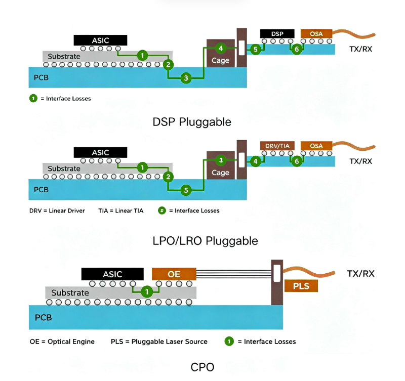
Architectural Differences
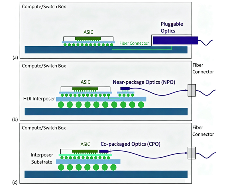
The core distinction between the two lies in the depth of physical coupling, at the packaging level, between the silicon photonics engine and the network switching ASIC.
CPO pursues seamless integration to the extreme. It employs advanced semiconductor packaging techniques to directly integrate the silicon photonics engine and the switching ASIC onto the same multi-chip substrate. This design compresses high-frequency electrical signal traces to just a few millimeters, thereby drastically mitigating, at the source, the severe signal attenuation typically caused by transmission media in high-speed channels.
NPO, by contrast, strikes a balance between signal integrity and system decoupling. Rather than forcibly encapsulating photonic devices within the ASIC's dedicated substrate, it packages them independently on high-performance sub-substrates and positions them in close proximity to the core chip. This approach significantly shortens trace lengths while maintaining the fundamental requirement of physical isolation between optical and electrical components.
The Engineering Dilemma of CPO
In theory, CPO (Co-Packaged Optics) represents the future evolution of optical interconnects, offering the industry's lowest power consumption and highest throughput density thanks to ultra-short electrical links. However, as the technology moves toward mass production, this deep physical integration faces formidable engineering challenges.
Complex yield control and manufacturing costs constitute the primary hurdles for CPO. A switching ASIC contains billions of transistors; under the CPO architecture, it is inextricably linked with precision optoelectronic components. This high level of integration means that if even a single optical channel fails, the complexity of fault isolation, testing, and repair for the entire system increases exponentially, severely dragging down manufacturing yields.
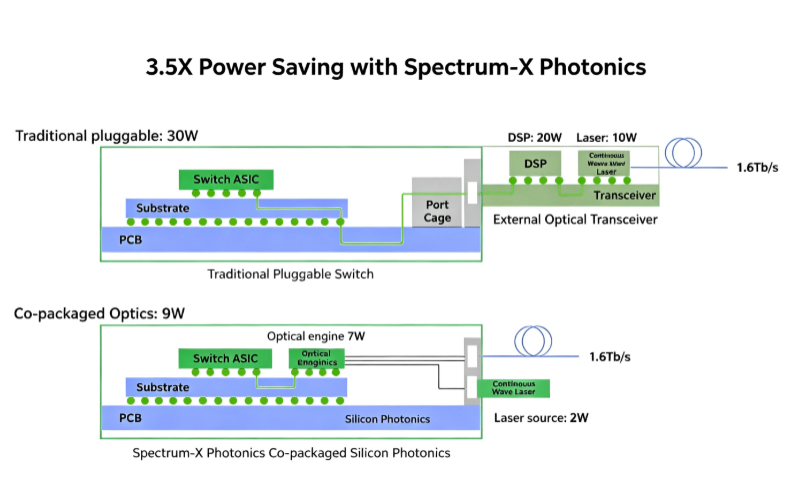
The unavoidable issue of thermal coupling presents another difficult challenge. High-throughput ASICs serve as the system's primary heat sources, whereas photonic devices are extremely sensitive to temperature drift. Forced co-packaging subjects optical components to prolonged exposure to extreme heat, easily triggering spectral drift and causing system bit errors. To mitigate this thermal interference, equipment vendors are forced to incur substantial costs for redundant designs in liquid-cooling cold plates.
The Pragmatic Advantages of NPO
Addressing the engineering challenges associated with CPO, NPO mitigates the risks of deep coupling through topological reconfiguration, thereby achieving high feasibility for mass production within the current supply chain ecosystem.
By maintaining physical separation, NPO enables contract manufacturers to conduct independent yield testing on the switching ASIC and the optical engine. Compared to highly integrated CPO, NPO offers greater operational latitude and design flexibility regarding component assembly, fault localization, and long-term system maintenance, effectively avoiding prohibitive maintenance costs.
Furthermore, this physical separation provides independent heat dissipation paths for high-heat-generating chips and silicon photonic engines. When combined with an external laser source design, NPO ensures that critical, sensitive components, such as lasers, operate in a stable, cool zone, thereby significantly extending their physical lifespan.
Regarding the critical metric of energy efficiency, NPO drastically reduces the length of signal traces, which traditionally span over ten centimeters, where signal loss occurs. Communication links no longer rely heavily on high-power DSP chips for extensive signal retiming; instead, they can utilize lightweight solutions such as low-power direct drive, effectively lowering the overall operating power consumption per port.
Diverging Application Scenarios
In terms of application scenarios, the two technologies have diverged significantly due to their differing levels of technical maturity and original design objectives.
NPO represents a highly practical transitional solution. It balances the urgent need to overcome the "power wall" with the feasibility of existing electronics manufacturing ecosystems; it aligns perfectly with current 1.6T applications and the upcoming early 3.2T nodes, making it a pragmatic choice for the smooth evolution of mainstream AI computing centers.
CPO, on the other hand, represents the ultimate future-oriented goal. It targets the ultra-high-speed 3.2T to 6.4T nodes of the future, and its implementation relies heavily on hyperscale computing clusters, specifically those with extremely stringent power consumption requirements and comprehensive, system-wide liquid cooling infrastructure.
Conclusion
In the quest to reduce high power consumption, CPO outlines the ultimate blueprint for extreme density and ultra-low power, while NPO, leveraging the engineering ingenuity of physical topology decoupling, ingeniously resolves the yield and thermal management challenges currently facing the industry. For AI data centers rapidly advancing toward the 1.6T era, NPO is by no means a mere stopgap compromise; rather, it represents a vital pathway, possessing immense engineering value and commercial viability, that computing power networks must traverse before fully transitioning to a co-packaged optics architecture.


share

