


Silicon Photonics and CPO Break 1.6T Network Limits

Silicon photonics and co-packaged optics are reshaping the interconnect infrastructure of AI data centers for the 1.6T era. As the scale of large-model training expands, the demand for ultra-high bandwidth within GPU clusters is becoming increasingly urgent. Traditional pluggable optical modules, as they evolve toward higher frequency ranges, are hitting physical limits regarding thermal and electrical performance, thereby becoming a critical bottleneck that constrains the full realization of computing power. The accelerated commercial adoption of silicon photonics and CPO technologies is poised to fundamentally break through the power consumption barrier for next-generation intelligent computing networks.
Power Consumption Limits of Pluggable Optics
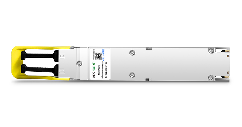
Traditional pluggable optical modules have dominated computing networks to date due to their deployment flexibility; however, as single-lane data rates surge to 224 Gbps PAM4, the electrical limitations inherent in their traditional physical architecture have become glaringly apparent.
In networks utilizing traditional optical modules, high-speed electrical signals must travel from the switching chip across PCB traces on the mainboard—spanning over ten centimeters—to reach the front panel. At these speeds, the signal's Nyquist frequency reaches 56 GHz; over such distances, high-frequency signals suffer from severe skin effect and dielectric loss, with channel insertion loss frequently exceeding 30 dB.
To compensate for the resulting extreme signal attenuation and distortion, traditional optical modules must integrate high-performance DSP chips for digital signal processing. This significantly increases the module's physical size and power consumption. At the 1.6T node, the power consumption of a single module approaches 30 W. If a 102.4T core switch is fully populated with 1.6T optical modules, the heat generated by the optical interconnects alone amounts to several kilowatts. Such extreme heat flux density renders traditional air-cooling solutions unsustainable, while the cold-plate layout and piping design for liquid-cooling systems present immense engineering challenges.
Architectural Evolution of Silicon Photonics and CPO
To overcome the physical limitations imposed by motherboard routing, silicon photonics and Co-Packaged Optics architectures offer a breakthrough solution by enhancing device integration and shortening electrical interconnects.
Traditional optical modules rely on assemblies of discrete optical components, resulting in bulky packaging and high optical signal loss. In contrast, silicon photonics leverages mature CMOS semiconductor processes to highly miniaturize and integrate modulators, detectors, and passive waveguides onto a single silicon-based chip. This fundamental restructuring of materials and processes eliminates the need for complex optical component stacking at the source, enabling extreme miniaturization of optoelectronic devices and ensuring high consistency in mass manufacturing.
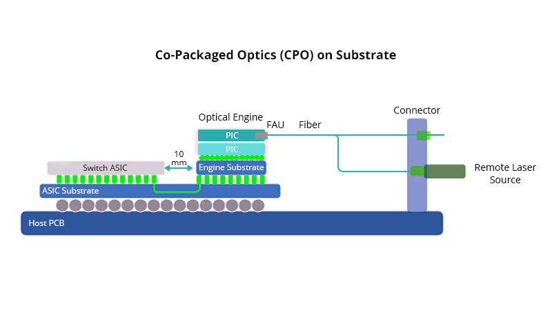
Building upon the high integration levels achieved by silicon photonics, CPO further reconfigures the physical topology of the equipment. CPO utilizes advanced packaging technology to co-package the silicon photonic engine and the network switching ASIC onto a single multi-chip substrate. This design drastically compresses the physical transmission path for high-speed electrical signals—reducing the distance from over ten centimeters on the motherboard to just a few millimeters within the substrate. These ultra-short interconnects significantly reduce channel attenuation, allowing the system to adopt a low-power linear direct-drive architecture and fundamentally eliminate reliance on power-hungry DSP chips.
System Energy Efficiency and Bandwidth Density
The shift from discrete components to highly integrated silicon-based solutions—and from long PCB traces to direct substrate-level interconnects—has fundamentally restructured the underlying architecture, yielding tangible, multi-dimensional system benefits.
The most immediate breakthrough is a significant reduction in energy consumption per bit transmitted. By eliminating power-hungry DSP chips, the CPO architecture cuts overall communication link power consumption by more than 30%. Simultaneously, removing the DSP eliminates the computational latency inherent in digital signal processing. In the context of collective communication for large-scale distributed training, this microsecond-level hardware pass-through capability drastically reduces synchronization wait times between nodes, effectively boosting the actual compute utilization of GPU clusters.
At the topology level, CPO completely frees up space on the switch's front panel. The front of the device no longer needs to accommodate bulky pluggable cages, retaining only high-density fiber-optic interfaces and external laser sources (ELS). This makes it feasible to achieve ultra-high switching throughput exceeding 102.4 Tbps within a 1RU form factor; this not only streamlines leaf-spine network hierarchies but also significantly reduces the complexity of fiber-optic cabling for clusters comprising tens of thousands of GPUs.
QSFPTEK 1.6T Silicon Photonics Solutions
During the transition toward CPO architectures, high-performance pluggable modules based on silicon photonics technology remain the practical foundation for scaling up computing power. To meet the demands of large-scale AI computing clusters, QSFPTEK has launched the 1.6T OSFP224 and 800G series of silicon photonics modules, utilizing a single-lane 224Gbps process. By employing highly integrated silicon photonic chips, these dual-rate products significantly reduce both the number of discrete components and operational power consumption. Backed by rigorous signal integrity testing, QSFPTEK’s entire high-speed silicon photonics lineup ensures stable, low-level interoperability with mainstream network equipment, facilitating a smooth transition for data centers to next-generation network architectures.
Conclusion
For network nodes operating at 1.6T and beyond, the traditional approach of trading increased electrical signal compensation for higher bandwidth has reached its physical limits. While high-speed pluggable modules—such as the 1.6T OSFP224—address immediate demands for scaling computing power, silicon photonics and co-packaged optics represent the key pathways to resolving long-term interconnect power consumption challenges. As silicon-based photonic integration and packaging technologies continue to mature, data center networks are steadily advancing into a new era of computing infrastructure reconfiguration characterized by architectural simplicity and high energy efficiency.


share

