


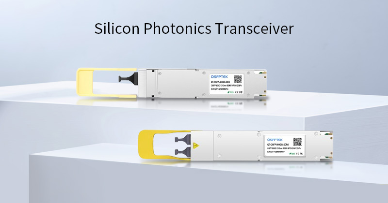
What Are Silicon Photonics (SiPh) Transceivers and Their Differences from Traditional Modules?

As data center speeds evolve toward 800G and even 1.6T, a technology known as Silicon Photonics (SiPh) is accelerating the transformation of optical module technology and reshaping the industry landscape. So what exactly is a Silicon Photonics transceiver? And in what fundamental ways does it differ from traditional optical modules?
The Evolution of Silicon Photonics Technology
From the proposal of integrated optics by Bell Laboratories in the United States in 1969 to the early 21st century, when companies such as Intel began entering the Silicon Photonics field to help drive technological breakthroughs, SiPh gradually moved into a stage of industrialization and technological acceleration. After 2008, companies including Luxtera and Intel started launching commercial silicon photonic integrated products, marking the formal entry of SiPh chips into the market. This laid the foundation for future high-speed optical modules, such as 400G and 800G modules.
The development of Silicon Photonics technology can be broadly divided into four stages. The first stage involves manufacturing the underlying components for optical communication using silicon-based materials, gradually replacing discrete optical components. The second stage sees the integration technology evolving from hybrid integration to monolithic integration, where various components are combined to achieve different functions on a single chip – this is the current state of SiPh technology. The third stage, in the future, is expected to achieve full optoelectronic integration through the fusion of optoelectronic technologies. And the fourth stage will involve decomposing devices into multiple silicon units arranged in a matrix-like fashion, allowing for programmable functionality through customized programming, resulting in programmable chips.
Silicon Photonics Optical Modules Overview
What is SiPh Optical Transceiver?
SiPh optical transceivers are optical modules based on Silicon Photonics technology. Before understanding silicon photonic modules, it is necessary to first clarify what Silicon Photonics technology is.
SiPh is a new-generation technology for developing and integrating optical devices using silicon and silicon-based substrate materials, such as SiGe/Si and SOI, by leveraging existing CMOS manufacturing processes.
The core concept behind silicon photonic modules is "replacing electricity with light," meaning that laser beams are used instead of electrical signals for data transmission. Silicon Photonics integrates the optical components and electronic elements within a SiPh optical transceiver onto a single, independent microchip, enabling deep integration of optical signal processing and electrical signal processing, and ultimately realizing true optical interconnects.
Advantages of Silicon Photonics Design
Firstly, for data centers requiring extensive use of optical modules, the most significant advantage of SiPh modules remains their low cost.
With the development of the internet industry, the demand for optical modules is increasingly shifting toward miniaturization and high performance. Under the miniaturization trend, conventional optical modules face increased performance degradation when attempting to boost transmission speeds. Silicon Photonics transceivers not only overcome performance bottlenecks like power consumption caused by multiple channels in conventional modules but also reduce laser costs.
In traditional module costs, the photonic chip represents about 40% of the total cost, while the laser contributes roughly 20%. Cutting laser costs by 75% can reduce the overall module cost by around 15%. By leveraging Silicon Photonics technology can achieve high integration of modulators and passive optical paths on a single chip, significantly reducing chip costs.
Low power consumption is another advantage of SiPh design. By replacing traditional electrical signals with optical signals for data transmission, Silicon Photonics technology effectively reduces energy consumption caused by resistive losses and signal attenuation during high-speed interconnects.
The third advantage is high integration and miniaturization. SiPh design utilizes CMOS technology to integrate multiple optical components such as modulators, detectors and waveguides onto a single silicon photonic chip, resulting in a smaller size, higher density, simplified packaging, and improved reliability.
Disadvantages of Silicon Photonics Transceiver
While Silicon Photonics modules have advantages in various aspects, they are still confronted with challenges at present technology level. These devices have low coupling efficiency between silicon waveguides and optical fibers, high losses, and are only suitable for short-to-medium distance transmissions. Furthermore, the integration of III-V compound materials on silicon substrates presents compatibility issues between the two materials, resulting in low wafer yield for SiPh chips. Finally, there is currently no cost advantage at data rates below 400G.
The Applications of the Silicon Photonics Module
Silicon Photonics modules are highly suitable for short-distance, high-bandwidth scenarios. GPU clusters in AI data centers require 800G or even 1.6T interconnects. The low power consumption and high density of Silicon Photonics modules can reduce TCO. Additionally, CPO technology enables zero-distance packaging of Silicon Photonics engines with switch chips, further reducing latency to meet the low-latency demands of AI training.
SiPh Module vs Traditional Transceiver Module, What's the Difference?
Technical Architecture and Materials
The mainstream technology path of the traditional optical module is "hybrid integrated", in which some key optical devices are still based on III-V compound semiconductor. For instance, InP is used in lasers and GaAs or LiNbO3 are used in modulators. These materials require complex assembly processes, including optical alignment, involving significant manual intervention. Taking a 100G traditional module as an example, it requires the alignment and packaging of more than ten components, including four 25G lasers, four modulators, and multiplexers/demultiplexers, involving over 30 process steps.
Siph modules use silicon as a base and etch optical waveguides, modulators, detectors, and other components onto a silicon wafer using CMOS semiconductor processes, achieving monolithic integration. This process is compatible with CPU manufacturing and can utilize mature production lines from companies like Intel for mass production, reducing the number of manufacturing steps by 60% and offering enormous potential for scaling up.
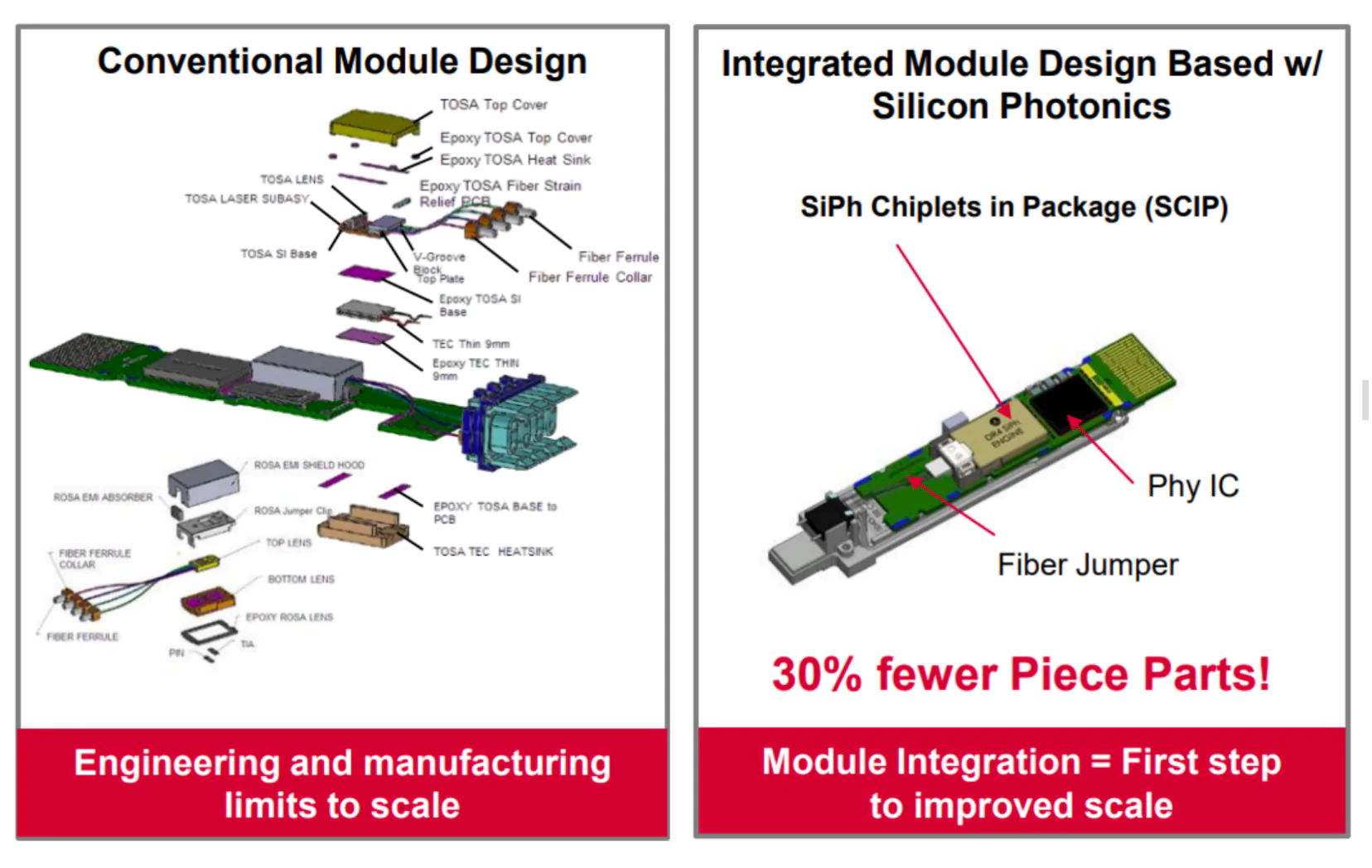
(Source: Broadcom)
Integration Density and Module Size
The integration of classic optical modules is hindered by material and precision challenges – to double the data rate, almost twice as many components would need to be combined. For instance, conventional 400G module consists of eight 50G channels which is much larger than that of a 100G module. In a 1U switch, a maximum of 32 traditional 400G modules can be deployed, pushing space utilization to its limits.
SiPh modules utilize photonic integration technology to compress dozens of optical components onto a 1cm² silicon chip. For example, an 800G Silicon Photonics module has a core chip the size of a fingernail, integrating eight 100G channels. This high-density characteristic allows a 1U switch to deploy 64 800G ports, doubling the bandwidth density and perfectly meeting the high-bandwidth demands of data centers.
Cost and Scalability
Traditional optical modules, most of which are manually aligned, packed and tested, especially for high-speed products where precision requirements are extremely high, leading to persistently high costs. This technological approach faces limitations as it attempts to scale to even higher data rates.
In contrast, the manufacturing process of silicon photonic modules is compatible with mature CMOS integrated circuit processes. This allows them to leverage the existing, large-scale semiconductor supply chain to achieve mass, standardized production. Once the technology reaches maturity, silicon photonic modules offer substantial cost-reduction potential and can more easily evolve toward higher data rates and more complex functionalities, providing excellent scalability.
Performance Characteristics
Traditional optical module technology is mature, offering stable and reliable performance, and still holds irreplaceable advantages in specific application scenarios, such as ultra-long-distance transmission. Silicon Photonics modules have significant advantages in power consumption and integration. However, their lasers still require external coupling, which is one of the technical challenges. Nevertheless, with the development of CPO technology, power consumption and latency can be further reduced, which is precisely what future ultra-large-scale data centers will require.
Will 1.6T Silicon Photonics Enter Mass Production?
With the explosive growth of artificial intelligence, demand for high-speed optical modules has surged. Coupled with Silicon Photonics technology offering a more streamlined product architecture, leading optical module manufacturers have accumulated substantial technical expertise in Silicon Photonics chips and related technologies while maintaining continuous investment. Consequently, modules based on Silicon Photonics technology are increasingly favored by data centers. As the Silicon Photonics supply chain continues to mature, 1.6T SiPh modules are expected to move toward large-scale deployment around 2025. In addition, we need to note that the mass production of 1.6T Silicon Photonics optical modules is not merely a breakthrough in a single technology, but a system-level coordinated breakthrough involving a series of cutting-edge technologies, including optical chips, electrical chips, packaging processes, materials science, and thermal management. This also implies that the number of manufacturers capable of competing in the 1.6T market will be significantly fewer than in the 800G era, with industry barriers being substantially raised.
The Future Market of Silicon Photonics Transceivers
According to the latest forecast from Yole Intelligence, the Silicon Photonics module market is entering a phase of rapid growth. By 2029, global sales of Silicon Photonics modules are expected to reach $10.3 billion.
Among them, pluggable Silicon Photonics modules for data centers account for the largest share, with projected revenue of approximately $5.3 billion, representing 52% of the total market. Silicon Photonics modules for WDM applications are expected to generate around $4.6 billion in revenue, accounting for 45% of the market. In addition, market segments such as data center optical I/O interfaces, NPO & CPO architectures, telecom wireless, and other applications are also gradually expanding, together contributing more than $200 million in market revenue.
According to Yole data, in terms of shipments, global Silicon Photonics module shipments have already reached nearly 6 million units in 2024, and are expected to exceed 12.5 million units in 2025, and potentially reach 18 million units by 2029.
Conclusion
Silicon photonics optical modules combine the strengths of photonics and CMOS technology, enabling lower costs, higher integration, and improved thermal and bandwidth performance. They are becoming a key solution for addressing the demands of high-performance computing, large-scale AI training, and telecommunications interconnects.


share

